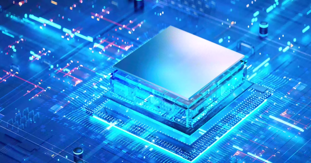
For decades, the semiconductor industry relied on Moore’s Law—the idea that the number of transistors on a chip doubles roughly every two years—to keep improving product performance. But as transistor designs approach atomic scales, traditional scaling is becoming extremely complex and expensive.
Enter advanced packaging: novel packaging integration architectures that rethink how chips are designed and connected. These technologies provide new ways to add more chip functions and optimize interconnect densities in a single package, bringing semiconductor components physically closer together to unlock computing, latency, power and cost benefits.
Why does this matter? Because today’s workloads—AI, high-performance computing (HPC) and next-generation devices—demand massive processing power at lightning speed. Advanced packaging makes that possible.
Let’s explore five key technologies driving this transformation.