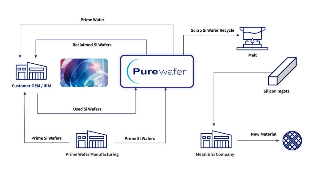
Each wafer undergoes detailed inspection and sorting, followed by precision lapping and etching to remove surface defects. Advanced polishing and cleaning restore the wafer to a high-quality, production-ready state. A final inspection ensures full compliance with customer specifications.
Wafers are then packaged in contamination-free cassettes, double-bagged, and shipped with full yield documentation. Optional laser marking enables complete lifecycle traceability.