Thin Films

Thermal Oxidation

Thermal Oxidation

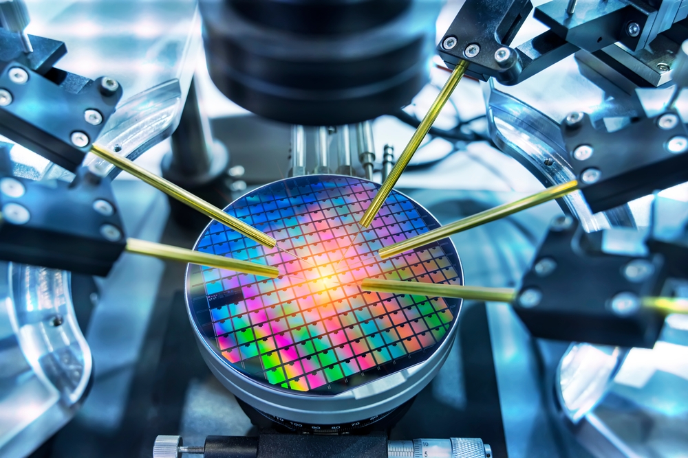
High-Uniformity Oxide Growth for Advanced Wafer Processing.

Pure Wafer provides precision thermal oxidation services for wafers from 100mm to 300mm, delivering the uniformity, control, and repeatability required for advanced semiconductor applications. Using tightly controlled horizontal furnace processes, we support both dry and wet oxidation across a broad range of oxide thicknesses.

  • 100mm to 300mm wafer support
  • 500Å to 10µm oxide thickness range
  • ±5% target thickness tolerance
  • ±3% within-wafer uniformity
  • Production-proven horizontal furnace capability

Process Specifications

CapabilitySpecification
Wafer Diameter100mm to 300mm
Oxide Thickness Range500Å to 10µm
Target Thickness Tolerance±5%
Within-Wafer Uniformity±3%
Standard Process Temperature1050°C
EquipmentHorizontal Furnace
Deposition TypeSteam / Double-Side
MetrologyFilmetrics

Dry vs. Wet Oxidation

Pure Wafer uses the right oxidation method based on the target film thickness and application requirements.

Oxide ThicknessProcess TypeBest For
Below 1000ÅDry OxidationCleaner, denser, more controlled thin oxides
Above 1000ÅWet OxidationFaster growth for thicker oxide layers
  • Dry oxidation offers superior film density, cleanliness, and control, making it ideal for thinner oxide growth.
  • Wet oxidation delivers a faster growth rate, making it the preferred solution for thicker oxides

For specialized applications, Pure Wafer can also develop combined dry/wet oxidation processes.

Engineered for Control

Advanced thermal oxidation performance depends on tightly managed process variables. Pure Wafer’s expertise includes control of:

  • Crystal orientation to optimize oxidation behavior
  • Dopant effects that influence growth rate
  • Chlorine enhancement for improved cleanliness and device performance
  • Pressure control to balance growth rate and temperature
  • Annealing Capability

In addition to oxidation, Pure Wafer offers nitrogen annealing to support downstream wafer performance and reliability.

Nitrogen Annealing Benefits

  • Relieves silicon stress
  • Activates implanted dopants
  • Reduces structural defects
  • Improves silicon-to-silicon dioxide interface quality
  • Bottom Web Callout

Precision oxidation. Tight uniformity. Production-scale reliability.

Schedule a Demo

Shop Test Wafers

Shop Prime Wafers

Precision Cleaning